For decades, the semiconductor industry followed a simple recipe: shrink transistors, put more of them on a single die, and performance improves. That recipe is running out of road. Advanced process nodes are extraordinarily expensive, large dies suffer from poor manufacturing yields, and moving data across a huge chip costs time and energy.
The industry's answer is to stop building only outward and start building upward and sideways, integrating multiple dies inside one package.
From 2D to 2.5D
In a traditional 2D design, every function sits on one monolithic die. In 2.5D integration, separate dies are placed side by side on a silicon interposer, a thin slice of silicon with extremely dense wiring. The interposer lets dies talk to each other far faster than they could through a normal package substrate.
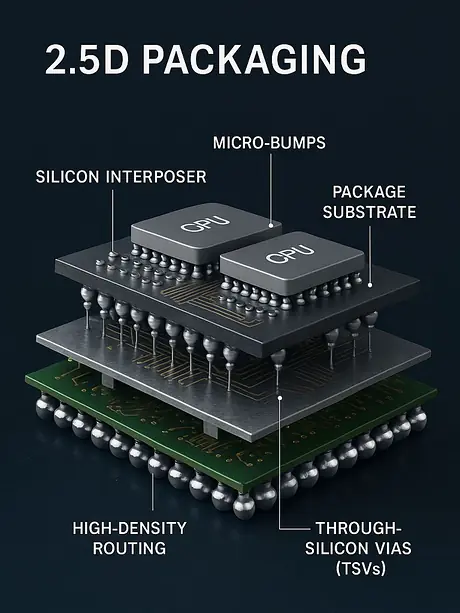
This is how many AI accelerators pair their compute die with stacks of High Bandwidth Memory (HBM), giving them the memory bandwidth modern workloads demand.
True 3D stacking
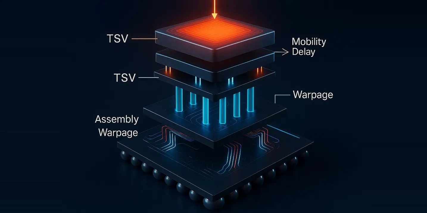
In 3D ICs, dies are stacked vertically and connected using through-silicon vias (TSVs) or hybrid bonding. Wires become microns long instead of millimetres, which cuts latency and power and makes much higher bandwidth possible.
Key idea: 3D integration shortens the distance data has to travel. In modern chips, moving data often costs more energy than computing on it.
2D
2.5D
3D
Chiplets
Chiplets: building chips like LEGO
A chiplet architecture splits a large design into smaller, modular dies. Each can be built on the process node that suits it best: leading-edge for compute, mature and cheaper nodes for I/O or analog. Standard die-to-die interfaces such as UCIe aim to let chiplets from different vendors work together in one package.
- Better yield: smaller dies mean fewer defects per die.
- Lower cost: only the parts that need the latest node use it.
- Reuse: proven chiplets can be combined into new products faster.
What this means for engineers
3D integration blurs the line between chip design and packaging. Engineers now need to think about partitioning a system across dies, thermal behaviour in a stack, signal and power integrity across interposers, and die-to-die interfaces. These skills are in growing demand, and they are exactly where BhavCore's consulting work is focused.
If you're starting a VLSI career, understanding advanced packaging is one of the best ways to stand out. Explore our packaging courses.